Semiconductor Manufacturing Challenge Simulator
Capital Investment ($B)
Amount spent annually on fab construction and equipment
EUV Tools Available
Number of extreme ultraviolet lithography machines
Skilled Workforce (Thousands)
Number of trained semiconductor engineers and technicians
Supply Chain Resilience
Degree of self-sufficiency in raw materials and components
Projected Global Capacity Share
Adjust sliders to see how changes affect the global distribution of chip production capacity.
Impact Summary
With current settings, U.S. production capacity would account for approximately 30% of global output, while Asia holds 40%. The U.S. needs to increase capital investment, EUV tool availability, and workforce size to close this gap.
Key Takeaways
- The U.S. faces a mix of cost, talent, and equipment hurdles that keep it behind Asia in chip output.
- Every advanced chip requires a "fab" that costs $10‑15billion plus ultra‑expensive lithography tools.
- The 2022 CHIPS Act injects $52billion, but funding alone won’t close the gap.
- Supply‑chain constraints on silicon, chemicals, and EUV machines limit rapid expansion.
- Strategic partnerships with TSMC, Intel, and Samsung are the fastest way for the U.S. to boost capacity.
When we talk about US semiconductor manufacturing the process of turning raw silicon into the tiny chips that power everything from smartphones to rockets, the answer isn’t “we don’t try.” The country spends billions, runs research labs, and even subsidises new fabs. Yet the output share still trails Taiwan, South Korea, and China. Below we break down why.
The Complex Nature of Semiconductor Production
Fabricating a modern 5‑nanometer processor means moving a wafer through more than 30 distinct steps-deposition, photolithography, etching, and inspection-inside a cleanroom that must stay under 10 particles per cubic meter. One misstep can ruin millions of dollars of work. This choreography is why a single fab can’t be built overnight.
Key entities in this workflow include:
- Lithography equipment machines that print circuit patterns onto silicon using extreme ultraviolet (EUV) light, supplied almost exclusively by ASML in the Netherlands.
- Cleanroom a climate‑controlled environment where dust‑free conditions protect delicate silicon surfaces.
- Supply chain raw materials like high‑purity silicon, photoresist chemicals, and specialty gases that travel across continents.
Each of these components forms a tightly woven network. Disrupt one link and the whole line stalls.
Capital Intensity & Equipment Bottlenecks
Building a cutting‑edge fab costs $10‑15billion, plus another $5‑7billion for EUV lithography tools-each tool exceeds $150million. These machines are so complex that only a handful of engineers worldwide understand how to maintain them.
ASML, the sole EUV supplier, caps production at about 20 machines per year. That limited supply creates a queue that can delay a new fab by 2‑3years, regardless of how much cash is on the table.
In contrast, Taiwanese firms like TSMC the world’s largest dedicated semiconductor foundry already own a fleet of over 150 EUV tools, giving them a massive production advantage.
Talent and Supply‑Chain Gaps
Even with fab space and machines, you need a deep pool of engineers, process technicians, and equipment specialists. The U.S. produces roughly 25,000 new semiconductor engineers each year, but a single fab can require 5,000‑8,000 highly trained staff.
Many of those experts are currently employed by Intel, which has been shedding jobs to cut costs, or by overseas fabs that lure talent with higher salaries and stock options.
Meanwhile, critical raw materials-germanium, gallium arsenide, specialty photoresists-are sourced mainly from Japan, South Korea, and Europe. Trade tensions can instantly raise prices or shut down shipments.
Policy Landscape - The CHIPS Act and Its Limits
In 2022 Congress passed the CHIPS Act a $52billion initiative to boost domestic semiconductor research, development, and manufacturing. The law promises grants for fab construction, tax credits for equipment purchases, and funding for workforce training.
So far, the act has funded:
- Intel’s $20billion expansion in Ohio.
- TSMC’s $12billion fab in Arizona.
- Samsung’s $17billion chip plant in Texas.
These projects will add roughly 30,000 wafers per month, but they still represent a fraction of global output-about 2‑3% of the world’s total capacity.
Why the shortfall? Funding is capped, and the application process takes up to 18months. Moreover, the act does not address the EUV bottleneck or the shortage of skilled technicians, both of which remain the biggest constraints.
Comparing U.S. and Asian Fab Landscapes
| Metric | United States | Taiwan & South Korea |
|---|---|---|
| Number of 5‑nm fabs | 1 (under construction) | 3 (operational) |
| Total EUV tools | ≈30 | ≈150 |
| Annual fab capex | $35billion | $90billion |
| Average wafer yield | ≈70% | ≈85% |
The numbers illustrate the scale gap. Even with rapid construction, U.S. capacity will likely lag behind the combined output of Taiwan’s TSMC and South Korea’s Samsung for the next decade.

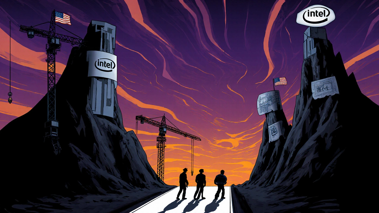
Recent Moves - Intel, TSMC, and Samsung in the U.S.
All three major players are betting on an American foothold:
- Intel the oldest U.S. integrated device manufacturer is shifting from a traditional PC‑focused roadmap to advanced 7‑nm and 5‑nm processes, pouring $20billion into a new fab complex in Ohio.
- TSMC is building a 5‑nm fab in Arizona slated for 2027, hoping to serve U.S. automotive and defense customers who need secure supply.
- Samsung the South Korean memory giant that also produces logic chips announced a 300‑mm fab in Texas, targeting AI accelerators.
These projects will create jobs, but they also rely on imported EUV tools and foreign expertise-so the U.S. still imports the critical heart of the operation.
Path Forward - What It Takes to Scale
Boosting domestic output isn’t just about money. A realistic roadmap includes:
- Secure more EUV capacity. The U.S. could negotiate joint ventures with ASML or fund a domestic R&D center for next‑generation lithography.
- Expand the talent pipeline. Community colleges, apprenticeship programs, and immigration pathways for skilled engineers must be accelerated.
- Build a resilient supply chain. Stockpiling critical chemicals, diversifying silicon sources, and encouraging domestic production of photoresist will reduce bottlenecks.
- Align policy incentives. Grants should be tied to measurable milestones-like installing a certain number of EUV tools-rather than just construction completion.
- Foster public‑private partnerships. Universities can host pilot fabs that serve as testing grounds for new processes before scaling to full production.
By addressing equipment scarcity, talent gaps, and supply‑chain fragility together, the U.S. can gradually climb from a 2‑percent share to a more strategic foothold in the global chip arena.
Frequently Asked Questions
Why is lithography the biggest bottleneck for U.S. fabs?
EUV lithography prints circuit patterns that are smaller than 10nanometers. Only ASML makes machines that can do this, and each tool costs over $150million. The limited production rate means even wealthy companies have to wait years for a slot.
How does the CHIPS Act differ from previous U.S. semiconductor policies?
Earlier policies focused mainly on research grants. The CHIPS Act adds direct manufacturing subsidies, tax credits for equipment, and workforce development funds, aiming to cover the whole fab ecosystem.
Will building more fabs solve the talent shortage?
Not on its own. A fab can create thousands of jobs, but the specialized roles require years of training. Without parallel investment in education and immigration, new plants will struggle to find qualified staff.
How do geopolitical tensions affect U.S. chip supply?
Tensions can restrict the flow of raw materials from East Asia or limit access to EUV machines. The U.S. has responded by creating strategic reserves and encouraging allied countries to diversify sources.
What role do foreign fabs like TSMC play in U.S. technology security?
TSMC’s Arizona plant aims to provide a domestic source for high‑security chips used in defense and aerospace, reducing reliance on overseas fabs that could be vulnerable to export controls.